DIT
DIT
News
Events
Organisation & contact
Campus locations
Campus Deggendorf
European Campus Rottal-Inn
Campus Cham
Unternehmerische Hochschule
Entrepreneurship Education
Startup Support
Scaling and Growth Support
Innovation Ecosystem
Job vacancies
Application Process
Become a professor
Impressions
International
Welcome Centre
Heroes
Gesunde Hochschule
Publications
Profile
Associates
Quality Management
University law
Alumni
Alumni Konferenz
Press
Deggendorf Institute of Technology in simple language
ESGRC
Location and directions
Follow us:
Study with us
Study with us
Why study at DIT
Course choices
Fields of study
Bachelor
Master
Cooperative Studies
Programmes in English
Discover and connect
How to apply
Events
International exchange students
School visit programmes
DIT for everyone
Studying and Living
Advice & Support
FAQs
Centre for studies
Subject Support
Info for parents
Prep courses
Find your Master
Ask the student
Funding your studies
Follow us:
Students
Students
A-Z
Faculties
Information for freshers
IT services
Language Centre
Organisation & documents
Application and Service fees for non-EU/EEA international applications and Service Fees
Career
Library
Campus life
Work & study abroad
International students
After graduation
Teach
Advice and support
Follow us:
Research
Research
Main areas of research
Research groups
Digital Security
Institutes
Institute for Precision Machining and High Frequency Technology
Fraunhofer Application Center
Institute for Quality and Material Analysis für Qualitäts- und Materialanalysen
Institute Future Technologies
Institute I-ETOS
Research locations
Campus Grafenau
Campus Parsberg/Lupburg
Campus Spiegelau
Campus Teisnach Optics
Campus Teisnach Sensor Technology
Campus Cham - Intelligent Production
Cham Campus - Intelligent Robotics
Campus Bad Kötzting
Campus Hutthurm
Campus Vilshofen
Campus Oberschneiding
Transformation Lab
Campus Wörth-Wiesent
Campus Mainburg
Campus Kemnath
Campus Freyung
Events
Expert symposium – future mobility
Day of Research
Projects
Labs
Scientific publications
Research funding
Doctorate
Research and Dissertation Competence
Digitech Doctoral Centre
Prisma Health Doctoral Centre
Follow us:
Professional Education
Professional Education
Bachelor
Master
Certificates
Informations and apply
MBA
Flexible booking of modules
Follow us:
Business
Business
Science for Business
Recruiting
Sponsoring and donating
STEM in the Region
Job Shadowing
Employer Branding with Professional Education
Follow us:
Follow us:
DE
EN
Logout
Zurück
Startseite
>
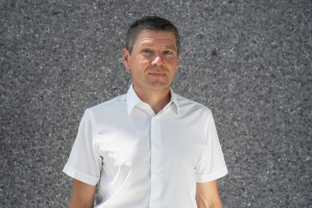
Prof. Dr.-Ing. Günther Benstetter
Institutes
Institute for Quality & Material Analysis
Director
E 208
0991/3615-513
publications
Sortierung:
Date
Typ + Datum
Publications loading
Search
Delete all filters